Bob Ayers
New Member
- Joined
- Aug 28, 2007
- Messages
- 2,274
- Reaction score
- 16
- Points
- 0
- Location
- Durham, NC
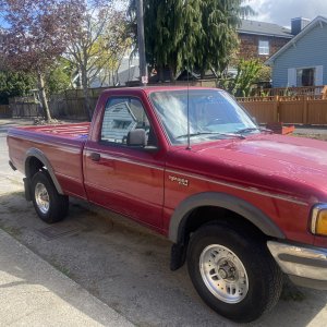
- Vehicle Year
- 1999
- Make / Model
- Ranger
- Transmission
- Automatic
While working for IBM, I developed, and taught a semiconductor (microelectronics) course. One of my "show and tells" was a P7 CPU chip (wafer, and modules). The P7 was developed by IBM in 2009, using a 45nm (nanometer) technology. 45nm is the minimum feature size (poly width) for the chip design. The P7 successor is the P8 CPU.
Here are some photos, that I thought would be of interest. The DOF is extremely shallow in some of the photos, even at f/22.
1 300mm silicon wafer. Red rectangle is one of many P7 CPU chips on the wafer.

2 Closer image of P7 CPU chip.

3 P7 CPU chip size comparison to penny.

4 Magnified edge of P7 CPU chip.

5 Magnified edge of P7 CPU chip.

6 Eye of needle used for size reference. Spherical shapes are solder balls used for I/O, power, and ground connections to chip.

7 Black rectangle is backside of “diced” chip attached to ceramic substrate. Chip solder balls are reflowed to attach chip to ceramic substrate.

8 Edge of ceramic substrate.

9 Bottom of ceramic substrate. Gold pads are for chip connections to socket/card.

10 Top of completed module.

11 Edge of completed module.

12 Bottom of completed module.

Here are some photos, that I thought would be of interest. The DOF is extremely shallow in some of the photos, even at f/22.
1 300mm silicon wafer. Red rectangle is one of many P7 CPU chips on the wafer.
2 Closer image of P7 CPU chip.
3 P7 CPU chip size comparison to penny.
4 Magnified edge of P7 CPU chip.
5 Magnified edge of P7 CPU chip.
6 Eye of needle used for size reference. Spherical shapes are solder balls used for I/O, power, and ground connections to chip.
7 Black rectangle is backside of “diced” chip attached to ceramic substrate. Chip solder balls are reflowed to attach chip to ceramic substrate.
8 Edge of ceramic substrate.
9 Bottom of ceramic substrate. Gold pads are for chip connections to socket/card.
10 Top of completed module.
11 Edge of completed module.
12 Bottom of completed module.